We develop, improve, simulate and test electronic circuits.
At the example of an electronic filter which is relatively simple and built up discreetly we show our possibilities for you in electronic circuit simulation:
Wiring statement
Functional description
The analysed circuit is a frequency lock. This kind of wiring is a part of this filter. The frequency lock has the characteristic to suppress a signal which a specific frequency the so-called resonant frequency. This circuit is therefore a selective network or a filter. It switches the input signal about a transistor circuit which works as impedance transformer on an alternating current bridge circuit (in Germany called Wienfilter). The other signals are then brought to the exit about another, complementary transistor circuit. The analysed frequency lock shows no reinforcements. The analysed network represents an economical alternative to conventional, passive R L C filters. The wiring was conceived to keep away disturbing net-grumble signals (50 Hz) of receiving plants. In principle this wiring has to be connected parallel to an entrance with a LC series resonant circuit.
Wiring simulation
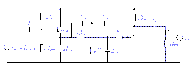
The frequency response shows the course of the output voltage into dependence of the frequency. This one represented here in the area of 10 Hz to 1 MHz.
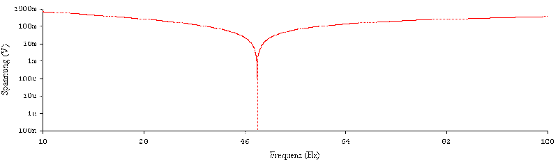
Phase
The highest stop-band attenuation
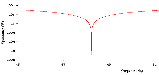
The wiring reaches the area of its highest stop-band attenuation at approx. 50 Hz (area) of 45 Hz to 50 Hz. The frequency range is approx. 300 Hz.
Summary
The operating point data of the transistors show approx. 30% change in the examined temperature range (27 degrees centigrade to 85 degrees centigrade).
The power consumption of the wiring is about 17 mW in the rest condition.
The knot tensions are largely temperature independent. The temperature influence on the emitter voltage at transistor Q1 makes itself noticeable by the fact that the tension as of approximately 100 Hz initial frequency is constant 4 mVs less.
The temperature variation doesn't have considerable influence on transistor Q2. The frequency response of the wiring is like that one of an R L C lock with a resonant frequency at 48.23 Hz.
The selection of the signal is carried out by a twin-t-filter. The recession of the wanted signals turns out surprisingly low.
The phase response reaches a maximum concerning the amount at resonant frequency.
The phase jump at resonant frequency is real and not a so called arc tangent fault.
The signals are to the input signal in phase.
The stop-band attenuation is 66 dB at resonance. The output voltage lies on sounding sine signal between 0 V and 9.6 V at a supply tension of 12 V.
The distortion factor is surprisingly high 57% for the scheduled 2 Vss signal with a frequency of 1 kHz. The selective effect of the wiring is based on the legitimacies of an alternating current bridge circuit.
The two transistors work as impedance transformers. By the relatively high initial resistance of both transistors (200 kOhm to 500 kOhm) the input signal or the bridge signal gets largely resilient for following amplifier stages.
The relatively low exit resistance of the common collector connections (100 ohms to 500 ohms) and the high current gain strengthen this trend.
There at semiconductors with -2,3s mVs/K or a decade's current increase per 16 K has to be calculated, the great thermal response also can be explained to the wiring.
The completely asymmetrical behaviour of the wiring at low frequency signals makes it necessarily to avoid such signals.
The high distortion factor is caused harmonic (1st harmonic wave) causally by the 2.
The filter is comparable with a Wien-Robinson .
A real Wien-Robinson filter would be more suitable here. The filter on hand is technical economically excellently suitable for the scheduled task reconcile improvements (not listed here).